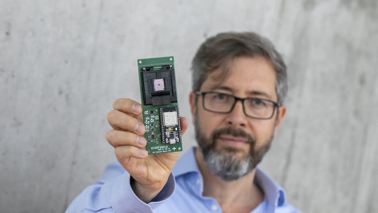
|
|
| |
prev/next
|
pubs
|
2009 |
2008 |
2007 |
2006 |
2005
|
2004
|
2003
|
2002
|
2001
|
2000
|
1999
|
1998
|
1997
|
1996
|
[back] |
269. |
Parallel arrays of Schottky barrier nanowire field effect transistors: Nanoscopic effects for macroscopic current output
Sebastian Pregl, Walter M. Weber, Daijiro Nozaki, Jens Kunstmann, L. Baraban, J. Opitz, Thomas Mikolajick, and G. Cuniberti
Nano Research 6, 381 (2013)
We present novel Schottky barrier field effect transistors consisting of a parallel array of bottom-up grown silicon nanowires that are able to deliver high current outputs. Axial silicidation of the nanowires is used to create defined Schottky junctions leading to on/off current ratios of up to 106. The device concept leverages the unique transport properties of nanoscale junctions to boost device performance for macroscopic applications. Using parallel arrays, on-currents of over 500 A at a source-drain voltage of 0.5 V can be achieved. The transconductance is thus increased significantly while maintaining the transfer characteristics of single nanowire devices. By incorporating several hundred nanowires into the parallel array, the yield of functioning transistors is dramatically increased and deviceto-device variability is reduced compared to single devices. This new nanowirebased platform provides sufficient current output to be employed as a transducer for biosensors or a driving stage for organic light-emitting diodes (LEDs), while the bottom-up nature of the fabrication procedure means it can provide building blocks for novel printable electronic devices.
| |
|
| |
prev/next
|
2009 |
2008 |
2007 |
2006 |
2005
|
2004
|
2003
|
2002
|
2001
|
2000
|
1999
|
1998
|
1997
|
1996
|
[back] |
|
| |
last modified: 2018.04.11 Mi
|
Prof. Dr. Gianaurelio Cuniberti
secretariat:
postal address:
Institute for Materials Science
TU Dresden
01062 Dresden, Germany
visitors and courier address:
|