| Funding period: | Oct. 1, 2019 to Sept. 30, 2022 |
| Agency: | DFG |
| Funding scheme: | International Cooperation |
| Further details: | https://gepris.dfg.de/gepris/projekt/405594721 |
We acknowledge funding by the DFG International Cooperation project "Straintronics of imperfect quasi-two-dimensional materials: coplanar vs lamellar heterostructures" (Straintronics, grant agreement ID: CU 44/43-1, AOBJ: 654782)
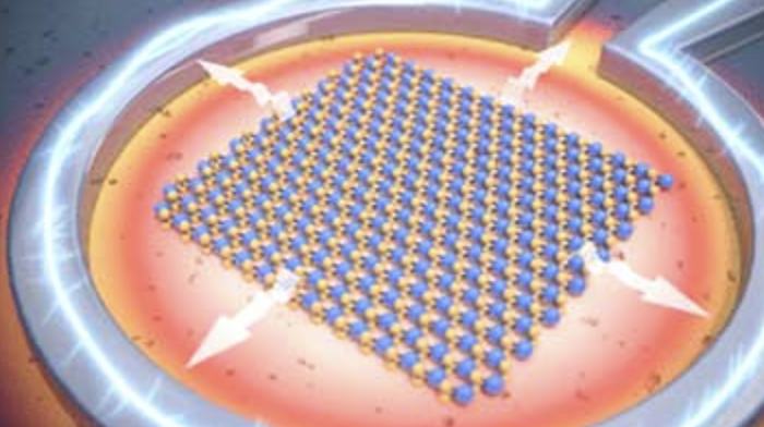
Over the past few years, the discovery of an increasingly large number of two-dimensional (2D) materials (besides graphene) has led to the emergence of a new experimental and theoretical research direction, whose goal is the exploitation of the fascinating electronic, structural, and transport properties of these 2D systems. Gaining control over those properties is clearly a pre-condition for the use of 2D materials in nanoelectronics, thermal or spintronics applications. In particular, nanoelectronic applications require the understanding of charge transport properties over various length scales as well as how electrical transport can be influenced by various extrinsic (electric, magnetic, light fields, etc.) or intrinsic (local and extended defects, surface functionalization, etc.) variables. In the current proposal, we combine the deep expertise of the two involved research groups in the modelling of charge transport in nanoscale systems to address the problem of strain and defect engineering in selected co-planar and lamellar heterostructures. For the sake of keeping a clear focus over the proposed funding period, we will limit ourselves to graphene and phosphorene heterostructures, although clearly other possibilities may be of interest. We combine atomistic quantum-transport approaches (TU Dresden, Germany) at the few-nanometers scale with real-space Kubo approaches (National Academy of Science, Ukraine) at a few hundreds of nanometers scale to elucidate the problem of how various types of defects (mostly vacancies, impurities, and grain boundaries) and (both homogeneously and inhomogeneously) applied strains can be used to tune charge transport in graphene/phosphorene heterostructures. The main links between both groups will consist in (i) the extensive parametrization of effective models to be used by the Ukrainian partner on the basis of the atomistic calculations to be performed by the German partner, (ii) the determination of possible meta-stable defect configurations within and in between the layers (by the German side) for subsequent calculations (by the Ukrainian side) of their effect on the electron diffusivity and electronic conductivity, and (iii) computer-aided design of nanoscale heterostructures with unique atomic configurations and shapeable (stretchable and flexible) structures with a potential for applications in nanoelectronics, magnetoelectronics, sensorics, etc. We expect that the results obtained within this project will not only have significance from the point of view of knowledge gain for both partners, but also be able to trigger appropriate experimental investigations in the field of straintronics of 2D materials and heterostructures in both the Department of Electronic Structure and Electronic Properties at the G. V. Kurdyumov Institute for Metal Physics of the N.A.S. of Ukraine and the Research Laboratory of Physical Materials Science of a Solid at the Taras Shevchenko National University of Kyiv.
| Funding period: | Oct. 1, 2019 to Sept. 30, 2022 |
| Agency: | DFG |
| Funding scheme: | International Cooperation |
| Further details: | https://gepris.dfg.de/gepris/projekt/405594721 |
We acknowledge funding by the DFG International Cooperation project "Straintronics of imperfect quasi-two-dimensional materials: coplanar vs lamellar heterostructures" (Straintronics, grant agreement ID: CU 44/43-1, AOBJ: 654782)
Over the past few years, the discovery of an increasingly large number of two-dimensional (2D) materials (besides graphene) has led to the emergence of a new experimental and theoretical research direction, whose goal is the exploitation of the fascinating electronic, structural, and transport properties of these 2D systems. Gaining control over those properties is clearly a pre-condition for the use of 2D materials in nanoelectronics, thermal or spintronics applications. In particular, nanoelectronic applications require the understanding of charge transport properties over various length scales as well as how electrical transport can be influenced by various extrinsic (electric, magnetic, light fields, etc.) or intrinsic (local and extended defects, surface functionalization, etc.) variables. In the current proposal, we combine the deep expertise of the two involved research groups in the modelling of charge transport in nanoscale systems to address the problem of strain and defect engineering in selected co-planar and lamellar heterostructures. For the sake of keeping a clear focus over the proposed funding period, we will limit ourselves to graphene and phosphorene heterostructures, although clearly other possibilities may be of interest. We combine atomistic quantum-transport approaches (TU Dresden, Germany) at the few-nanometers scale with real-space Kubo approaches (National Academy of Science, Ukraine) at a few hundreds of nanometers scale to elucidate the problem of how various types of defects (mostly vacancies, impurities, and grain boundaries) and (both homogeneously and inhomogeneously) applied strains can be used to tune charge transport in graphene/phosphorene heterostructures. The main links between both groups will consist in (i) the extensive parametrization of effective models to be used by the Ukrainian partner on the basis of the atomistic calculations to be performed by the German partner, (ii) the determination of possible meta-stable defect configurations within and in between the layers (by the German side) for subsequent calculations (by the Ukrainian side) of their effect on the electron diffusivity and electronic conductivity, and (iii) computer-aided design of nanoscale heterostructures with unique atomic configurations and shapeable (stretchable and flexible) structures with a potential for applications in nanoelectronics, magnetoelectronics, sensorics, etc. We expect that the results obtained within this project will not only have significance from the point of view of knowledge gain for both partners, but also be able to trigger appropriate experimental investigations in the field of straintronics of 2D materials and heterostructures in both the Department of Electronic Structure and Electronic Properties at the G. V. Kurdyumov Institute for Metal Physics of the N.A.S. of Ukraine and the Research Laboratory of Physical Materials Science of a Solid at the Taras Shevchenko National University of Kyiv.