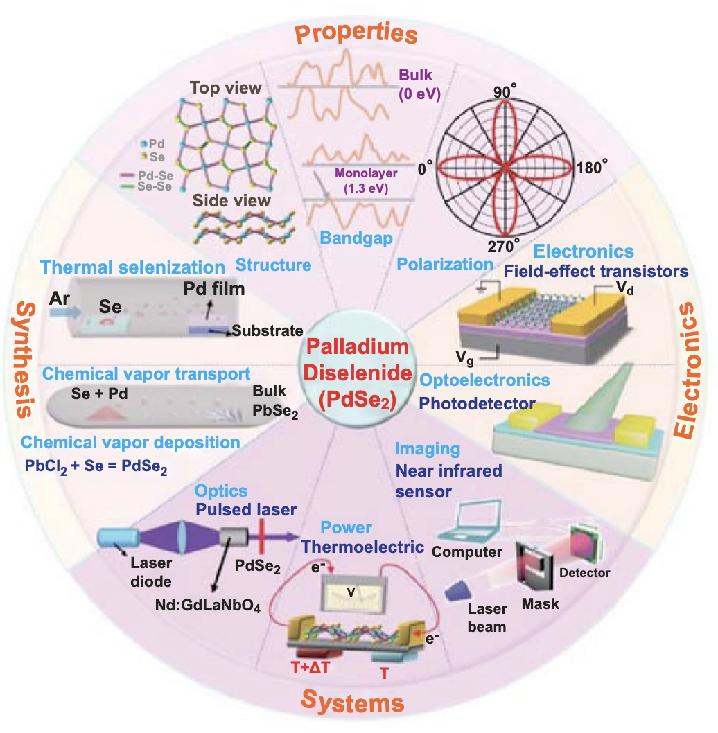
The rapid development of two-dimensional (2D) transition-metal dichalcogenides has been possible owing to their special structures and remarkable properties. In particular, palladium diselenide (PdSe2) with a novel pentagonal structure and unique physical characteristics have recently attracted extensive research interest. Consequently, tremendous research progress has been achieved regarding the physics, chemistry, and electronics of PdSe2. Accordingly, in this review, we recapitulate and summarize the most recent research on PdSe2, including its structure, properties, synthesis, and applications. First, a mechanical exfoliation method to obtain PdSe2 nanosheets is introduced, and large-area synthesis strategies are explained with respect to chemical vapor deposition and metal selenization. Next, the electronic and optoelectronic properties of PdSe2 and related heterostructures, such as field-effect transistors, photodetectors, sensors, and thermoelectric devices, are discussed. Subsequently, the integration of systems into infrared image sensors on the basis of PdSe2 van der Waals heterostructures is explored. Finally, future opportunities are highlighted to serve as a general guide for physicists, chemists, materials scientists, and engineers. Therefore, this comprehensive review may shed light on the research conducted by the 2D material community.
The rapid development of two-dimensional (2D) transition-metal dichalcogenides has been possible owing to their special structures and remarkable properties. In particular, palladium diselenide (PdSe2) with a novel pentagonal structure and unique physical characteristics have recently attracted extensive research interest. Consequently, tremendous research progress has been achieved regarding the physics, chemistry, and electronics of PdSe2. Accordingly, in this review, we recapitulate and summarize the most recent research on PdSe2, including its structure, properties, synthesis, and applications. First, a mechanical exfoliation method to obtain PdSe2 nanosheets is introduced, and large-area synthesis strategies are explained with respect to chemical vapor deposition and metal selenization. Next, the electronic and optoelectronic properties of PdSe2 and related heterostructures, such as field-effect transistors, photodetectors, sensors, and thermoelectric devices, are discussed. Subsequently, the integration of systems into infrared image sensors on the basis of PdSe2 van der Waals heterostructures is explored. Finally, future opportunities are highlighted to serve as a general guide for physicists, chemists, materials scientists, and engineers. Therefore, this comprehensive review may shed light on the research conducted by the 2D material community.