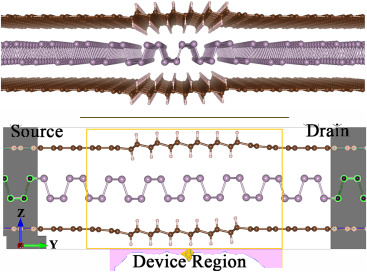
Chemical modification and vertical stacking of two-dimensional materials are promising techniques for new nanoelectronic devices. We present Density Functional Tight Binding (DFTB) calculations of a field-effect device, based on lateral and vertical heterostructures of 2D materials. The device consists of a phosphorene channel protected by graphene sheets, which work as contacts and are divided into the source and drain by local hydrogenation of graphene, which gives insulating graphane. In this device composed of only 3 layers, single sheets of graphene-graphane can work as both leads and oxide gate, while also acting as protective layers for a phosphorene channel. We show how for perfect vdW heterostructures of graphane/phosphorene/graphane and graphene/phosphorene/graphene the Schottky barrier is deeply influenced by normal electric fields, and we characterize electronic transport of such a device. Finally, we characterize phosphorene channel doping and defects, which, at very high densities in the transport direction, enables transport inside the phosphorene bandgap.
Chemical modification and vertical stacking of two-dimensional materials are promising techniques for new nanoelectronic devices. We present Density Functional Tight Binding (DFTB) calculations of a field-effect device, based on lateral and vertical heterostructures of 2D materials. The device consists of a phosphorene channel protected by graphene sheets, which work as contacts and are divided into the source and drain by local hydrogenation of graphene, which gives insulating graphane. In this device composed of only 3 layers, single sheets of graphene-graphane can work as both leads and oxide gate, while also acting as protective layers for a phosphorene channel. We show how for perfect vdW heterostructures of graphane/phosphorene/graphane and graphene/phosphorene/graphene the Schottky barrier is deeply influenced by normal electric fields, and we characterize electronic transport of such a device. Finally, we characterize phosphorene channel doping and defects, which, at very high densities in the transport direction, enables transport inside the phosphorene bandgap.