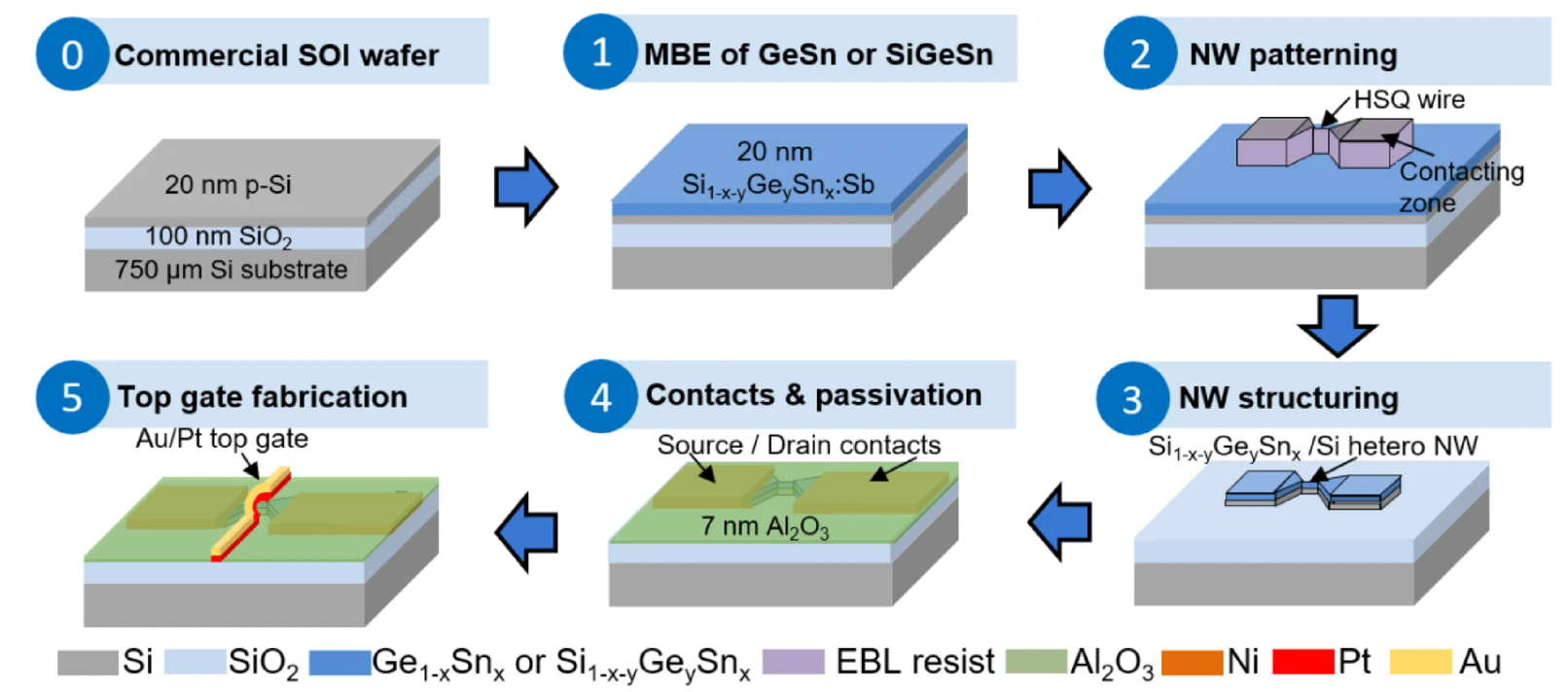
Ge1−xSnx and Si1−x−yGeySnx alloys are promising materials for future nanoelectronic applications owing to their high carrier mobilities and CMOS compatibility. However, ternary Si1−x−yGeySnx transistors have only theoretically been discussed, and there are only a few reports on lateral n-type Ge1−xSnx transistors to benchmark their material performance. The low equilibrium solid solubility of Sn in Si1−xGex (less than 1 at%) requires device fabrication processes at temperatures below the growth temperature of Si1−x−yGeySnx (x > equilibrium solubility) or at non-equilibrium conditions. Therefore, Si-based processes need to be adjusted according to the materials requirements. A relatively easy-to-fabricate device concept are junctionless field effect transistors, which operate as a gated resistor. In this work, we use Ge0.94Sn0.06 and Si0.14Ge0.80Sn0.06 grown on silicon-on-insulator substrates to fabricate and characterize lateral n-type Ge1−xSnx and SiyGe1−x−ySnx junctionless field effect transistors. The transistors were structurally characterized by top-view scanning electron microscopy and cross-sectional transmission electron microscopy. Electrical characterizations by transfer characteristics show the first working n-type Ge1−xSnx and Si1−x−yGeySnx hetero-nanowire transistors, achieving on/off-current ratios of up to eight orders of magnitude.
Ge1−xSnx and Si1−x−yGeySnx alloys are promising materials for future nanoelectronic applications owing to their high carrier mobilities and CMOS compatibility. However, ternary Si1−x−yGeySnx transistors have only theoretically been discussed, and there are only a few reports on lateral n-type Ge1−xSnx transistors to benchmark their material performance. The low equilibrium solid solubility of Sn in Si1−xGex (less than 1 at%) requires device fabrication processes at temperatures below the growth temperature of Si1−x−yGeySnx (x > equilibrium solubility) or at non-equilibrium conditions. Therefore, Si-based processes need to be adjusted according to the materials requirements. A relatively easy-to-fabricate device concept are junctionless field effect transistors, which operate as a gated resistor. In this work, we use Ge0.94Sn0.06 and Si0.14Ge0.80Sn0.06 grown on silicon-on-insulator substrates to fabricate and characterize lateral n-type Ge1−xSnx and SiyGe1−x−ySnx junctionless field effect transistors. The transistors were structurally characterized by top-view scanning electron microscopy and cross-sectional transmission electron microscopy. Electrical characterizations by transfer characteristics show the first working n-type Ge1−xSnx and Si1−x−yGeySnx hetero-nanowire transistors, achieving on/off-current ratios of up to eight orders of magnitude.