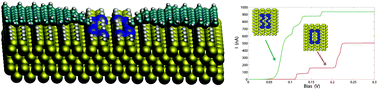
Dangling bond structures created on H-passivated silicon surfaces offer a novel platform for engineering planar nanoscale circuits, compatible with conventional semiconductor technologies. In this investigation we focus on the electronic structure and quantum transport signatures of dangling bond loops built on H-passivated Si(100) surfaces contacted by carbon nanoribbons, thus leading to a two-terminal planar, nanoscale setup. The computational studies were carried out to rationalize the influence of the local atomic-scale contacts of the dangling bond system to the mesoscopic electrodes as well as the possibility of revealing quantum interference effects in the dangling bond loops. Our results reveal a strong sensitivity of the low-energy quantum transmission to the loop topology and to the atomistic details of the electrode-loop contact. Varying the length of the loop or the spatial position of at least one of the electrodes has a drastic impact on the quantum interference pattern; depending on whether constructive or destructive interference within the loop takes place, the conductance of the system can be tuned over several orders of magnitude, thus suggesting the possibility of exploiting such quantum mechanical effects in the design of two-dimensional, atomic-scale electronic devices such as logic gates.
Dangling bond structures created on H-passivated silicon surfaces offer a novel platform for engineering planar nanoscale circuits, compatible with conventional semiconductor technologies. In this investigation we focus on the electronic structure and quantum transport signatures of dangling bond loops built on H-passivated Si(100) surfaces contacted by carbon nanoribbons, thus leading to a two-terminal planar, nanoscale setup. The computational studies were carried out to rationalize the influence of the local atomic-scale contacts of the dangling bond system to the mesoscopic electrodes as well as the possibility of revealing quantum interference effects in the dangling bond loops. Our results reveal a strong sensitivity of the low-energy quantum transmission to the loop topology and to the atomistic details of the electrode-loop contact. Varying the length of the loop or the spatial position of at least one of the electrodes has a drastic impact on the quantum interference pattern; depending on whether constructive or destructive interference within the loop takes place, the conductance of the system can be tuned over several orders of magnitude, thus suggesting the possibility of exploiting such quantum mechanical effects in the design of two-dimensional, atomic-scale electronic devices such as logic gates.