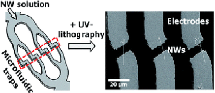
We present a simple method to microfluidically align and trap 1D nanostructures from suspension at well-defined positions on a receiver substrate for the fabrication of single-nanowire field effect transistors (NW FETs). Our approach allows for subsequent contacting of deposited NWs via standard UV-lithography. We demonstrate that silicon as well as copper(II) oxide NWs can be processed, and that up to 13 out of 32 designated trapping sites are occupied with single-NW FETs.
We present a simple method to microfluidically align and trap 1D nanostructures from suspension at well-defined positions on a receiver substrate for the fabrication of single-nanowire field effect transistors (NW FETs). Our approach allows for subsequent contacting of deposited NWs via standard UV-lithography. We demonstrate that silicon as well as copper(II) oxide NWs can be processed, and that up to 13 out of 32 designated trapping sites are occupied with single-NW FETs.