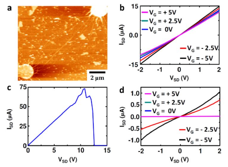
The exceedingly high current capacity of single wall carbon nanotubes (SWCNTs) and the high currents that SWCNT thin films can sustain are driving significant efforts to fabricate high quality horizontally aligned SWCNTs. Dielectrophoresis is being increasingly used to prepare aligned nanotubes. However, the aligned nanotubes are generally of low quality since the processing involved can introduce defects. In addition, in arrays of tubes, tube-tube contact resistance can be high. Electrostatic force microscopy is a technique similar to atomic force microscopy, but in this case a bias voltage between the conductive tip and sample enables one to probe the long range electrostatic force. In this study we confirm that the technique can be successfully used to spatially determine defects, crossover points between tubes and nanotube electronic type.

The exceedingly high current capacity of single wall carbon nanotubes (SWCNTs) and the high currents that SWCNT thin films can sustain are driving significant efforts to fabricate high quality horizontally aligned SWCNTs. Dielectrophoresis is being increasingly used to prepare aligned nanotubes. However, the aligned nanotubes are generally of low quality since the processing involved can introduce defects. In addition, in arrays of tubes, tube-tube contact resistance can be high. Electrostatic force microscopy is a technique similar to atomic force microscopy, but in this case a bias voltage between the conductive tip and sample enables one to probe the long range electrostatic force. In this study we confirm that the technique can be successfully used to spatially determine defects, crossover points between tubes and nanotube electronic type.
