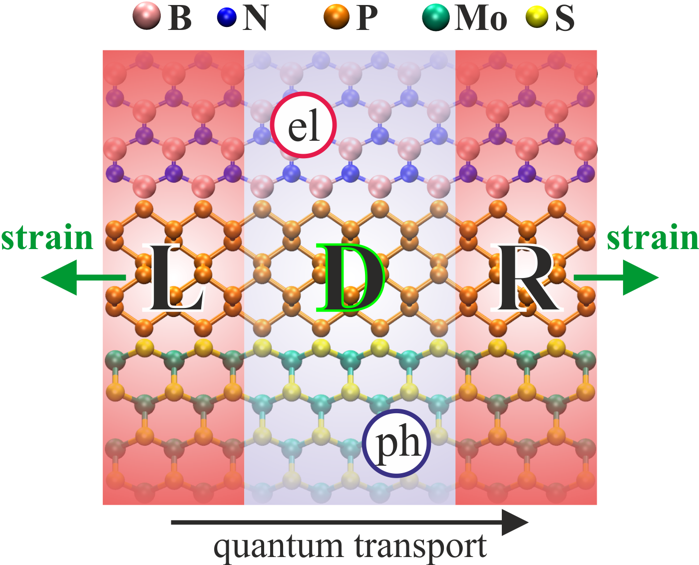
Novel two-dimensional (2D) materials show unusual physical properties which combined with strain engineering open up the possibility of new potential device applications in nanoelectronics. In particular, transport properties have been found to be very sensitive to applied strain. In the present work, using a density-functional based tight-binding (DFTB) method in combination with Green’s function (GF) approaches, we address the effect of strain engineering of the transport setup (contact-device(scattering)-contact regions) on the electron and phonon transport properties of two-dimensional materials, focusing on hexagonal boron-nitride (hBN), phosphorene, and MoS2 monolayers. Considering unstretched contact regions, we show that the electronic bandgap displays an anomalous behavior and the thermal conductance continuously decreases after increasing the strain level in the scattering region. However, when the whole system (contact and device regions) is homogeneously strained, the bandgap for hBN and MoS2 monolayers decreases, while for phosphorene it first increases and then tends to zero with larger strain levels. Additionally, the thermal conductance shows specific strain dependence for each of the studied 2D materials. These effects can be tuned by modifying the strain level in the stretched contact regions.
Novel two-dimensional (2D) materials show unusual physical properties which combined with strain engineering open up the possibility of new potential device applications in nanoelectronics. In particular, transport properties have been found to be very sensitive to applied strain. In the present work, using a density-functional based tight-binding (DFTB) method in combination with Green’s function (GF) approaches, we address the effect of strain engineering of the transport setup (contact-device(scattering)-contact regions) on the electron and phonon transport properties of two-dimensional materials, focusing on hexagonal boron-nitride (hBN), phosphorene, and MoS2 monolayers. Considering unstretched contact regions, we show that the electronic bandgap displays an anomalous behavior and the thermal conductance continuously decreases after increasing the strain level in the scattering region. However, when the whole system (contact and device regions) is homogeneously strained, the bandgap for hBN and MoS2 monolayers decreases, while for phosphorene it first increases and then tends to zero with larger strain levels. Additionally, the thermal conductance shows specific strain dependence for each of the studied 2D materials. These effects can be tuned by modifying the strain level in the stretched contact regions.